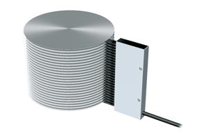
The wafer mapping sensor speeds up the sensing process while maintaining reliable detection.
ASW-SG625AP
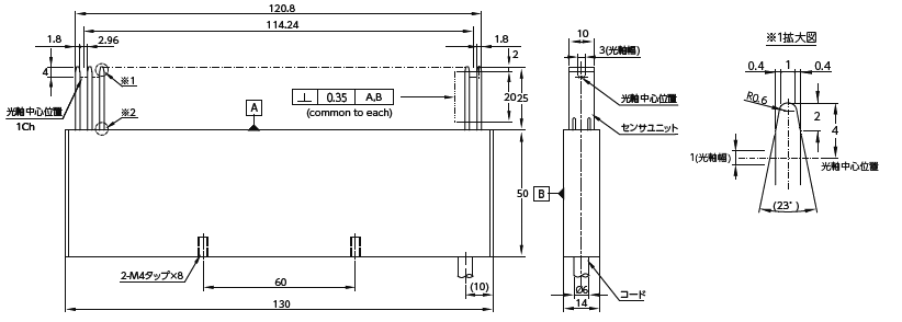
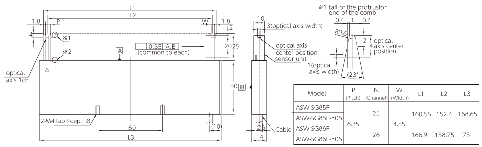
The dimension shown in these drawing apply to the bottom end (※2), not the protrusion end (※1) of the comb.
ASW-SG85F
ASW-SG85F-Y05
ASW-SG86F
ASW-SG86F-Y05
The dimension shown in these drawing apply to the bottom end (※2), not the protrusion end(※1) of the comb.
ASW-SG125VF
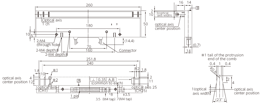
The dimension shown in these drawing apply to the bottom end (※2), not the protrusion end (※1) of the comb.
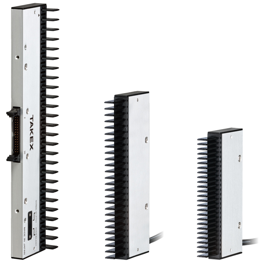
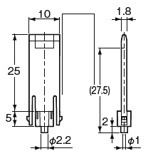
Comb sensor unit
ASW-F2500
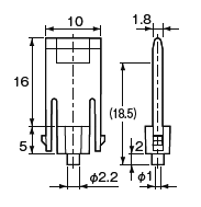
Comb sensor unit
ASW-F1600
ASW-SG625AP
ASW-SG85F
ASW-SG86F
ASW-SG85F-Y05
ASW-SG86F-Y05
ASW-SG125VF
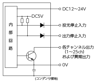
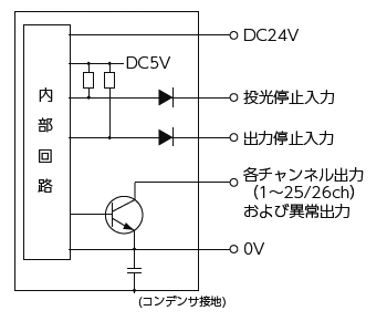
(For a noise prevention, a capacitor is installed between the 0V power supply and the sensor’s aluminum case.
Do not conduct withstand voltage Test between any input / output and the sensor case. )
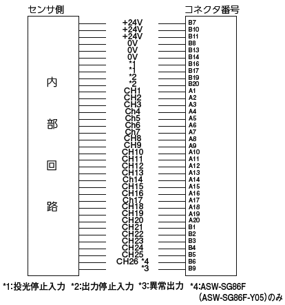
External wiring and connector number
| Semiconductor
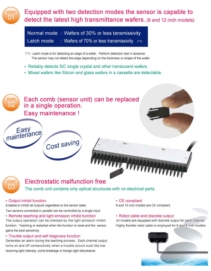
Collective Detection of Wafers
|
Presence of wafers in cassette collectively checked for mapping.
| Semiconductor
Detection of Translucent Wafers
|
Simultaneously detects all the translucent wafers etc. in cassette by latch mode. Through beam method is adopted for reliable detection.